The Integrated Circuits inspired by Wireless and Biomedical Electronic Systems (IC~WiBES) lab at Centre for VLSI and Embedded Systems Technologies (CVEST), IIITH is having its moment in the sun with a historic chip tape out as well as its selection into MeitY’s prestigious SMDP program.
If semiconductors are the lifeblood of the digital economy, then the lifeblood of semiconductors themselves is appropriate innovation fuelled by R&D. Understanding this only too well, the IC~WiBES research lab at IIITH has a strong R&D focus. But it also channels the innovations into applications that revolve around healthcare, high speed communication and quantum sensing. “We work on both IC (Integrated Chip) Design and System Design,” elaborates Prof. Abhishek Srivastava, founder of the IC~WiBES lab. On the chip design front, he emphasises that unlike mere designing on software, it is an actual chip that is being designed for specific applications. “We also perform measurements and build prototypes from our chips,” he continues, adding that his team develops different systems to address application areas. “We do that by using our own Application Specific Integrated Circuits (ASICS) which we design here or the commercially available off-the-shelf component-based systems.”
Over the last few years, the research lab has developed an IC characterization facility where through various projects and fundings, state-of-the-art equipment required to measure the performance of chips has been procured. Additionally, as part of the IC~WiBES lab, an electronic system design and test facility has also been established, where cost-based embedded systems development and testing can be carried out. A sensor fabrication facility too has been set up. “These facilities are being used not only by the institute but by interested parties from outside too,” remarks Prof. Srivastava.

Marking A Milestone
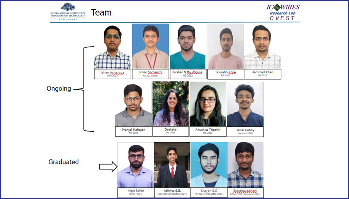
In the past, chip design and fabrication at the lab was typically undertaken in collaboration with other stakeholders, but a significant milestone was achieved with the designing and taping-out of a full test chip by a team of MS students at CVEST under the guidance of Prof. Srivastava. While a tape-out or fabrication is not novel in itself, it is definitely uncommon for academic institutions in India. “Only a few IITs and the IISc do it,” says the professor. The term “tape-out” owes its historic origins to the practice of recording the ASIC design files on magnetic tape which used to then be sent to the foundry for manufacturing. Today, in lieu of the magnetic tape, the design is often sent digitally, sometimes in GDSII (Graphic Design System II) format, to semiconductor fabrication plants for manufacturing. The research team fabricated the test chip in TSMC 65 nm technology. The chip includes advanced components crucial for modern communications, such as mmWave (near 20 GHz) and Sub-6 GHz circuits, which include receiver front end circuits, frequency synthesizers modules such Oscillator, Delta Sigma Modulator (DSM), frequency dividers, and filter. According to the group, these technological advancements are set to enhance the performance and efficiency of mmWave sensing, with potential impacts across healthcare systems. Explaining why the process of chip design and tape-out marks a crucial step in transitioning from theoretical designs to a manufacturable product, the professor states that it not only significantly advances the institute’s technological capabilities, it’s also crucial for enabling students and researchers to innovate, publish significant findings, and prepare for high-impact careers in the semiconductor industry.
 Patents for Prototypes
Some of the systems that have been developed at the IC~WiBES lab include one that can detect respiratory diseases in children. “A patent has been filed for this wireless pneumonia detector, even as it undergoes clinical trials,” reveals the professor. Another patent has been filed for a prototype of a safety device for factory workers that can detect abnormal heart rates, SP02, body temperature and falls, to enable emergency medical aid that is crucial in the golden hour. A radar-based healthcare application for capturing heart rate and breath rate data of multiple subjects simultaneously and non-invasively grabbed eyeballs recently at Iinventiv 2024 – a mega R&D fair for premier research and engineering institutes of the country. The group has also developed a prototype for road safety and security applications. For instance, it can classify and identify different objects on the road. “It is weather-agnostic, which means that even in dark, foggy, and rainy conditions, it can identify objects such as cars or bikes,” remarks Prof. Srivastava. The team is already working on extensions to the original systems that have been developed. Take the radar-based sensing of human gestures for one. “It is useful in scenarios where privacy is a concern like in a bathroom for example, where elderly monitoring can be undertaken via gesture recognition, posture recognition, and fall detection. Similarly, health monitoring in the form of non-invasive tracking of vitals can be extended to ADAS systems where both the driver’s and other occupants’ heart rates are displayed on the screen,” he explains.
A MeitY Move
Prof. Abhishek Srivastava’s project proposal titled, “Development of Silicon Proven IP Cores, Transceiver IC, and System Prototype for mmWave Radar Sensing in Healthcare and Security Applications’ has been selected for the prestigious Special Manpower Development Program for Chips to Startup (SMDP C2S) program by the Ministry of Electronics and Information Technology (MeitY). The C2S initiative is part of the Centre’s broader vision to foster next generation capabilities among chip designers for making India self-reliant in electronics system design. With the IIITH’s project aiming to develop a complete mmWave (24GHz) sensing technological platform in India, it represents a significant step forward in localised high-frequency technology development – something critical for enhancing India’s capabilities in strategic sectors such as healthcare and security.
According to the Professor, with this selection, IIITH will gain access to cutting-edge Electronic Design Automation (EDA) tools and state-of-the-art fabrication facilities. “These resources are essential for the development of advanced semiconductor devices and will prepare faculty and students to contribute significantly to India’s semiconductor knowledge pool. Plus, the institute’s participation opens new doors for collaboration with India’s leading academic institutions such as IITs, IISc, NITs, and other central and private universities which will foster a rich exchange of ideas, expertise and resources,” he muses.


Sarita Chebbi is a compulsive early riser. Devourer of all news. Kettlebell enthusiast. Nit-picker of the written word especially when it’s not her own.


Next post